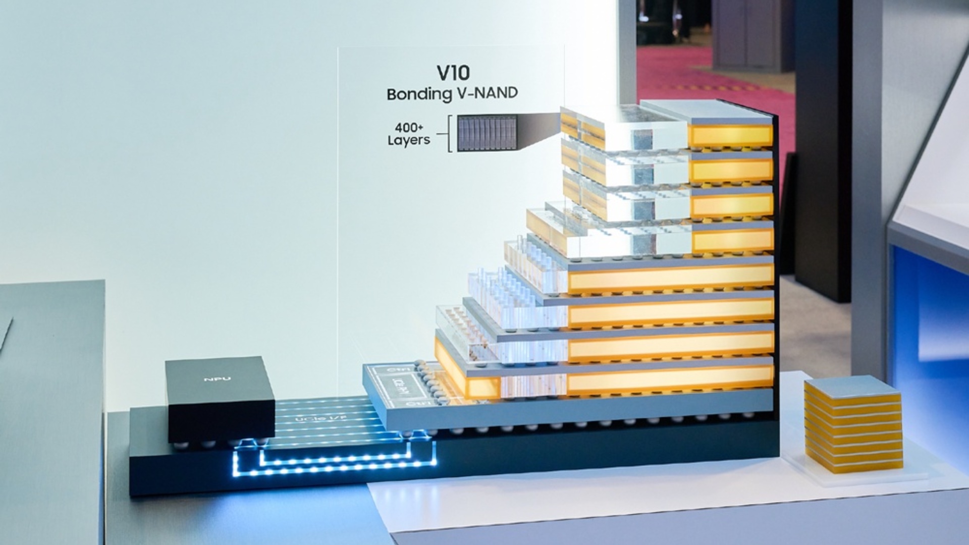

Alongside the zHBM concept, Samsung Electronics unveiled its V10 BV-NAND storage chip at the Future of Memory and Storage (FMS) 2026 expo today. It uses the company's 10th-generation vertical NAND flash memory architecture and represents a major technical upgrade over previous-generation NAND flash chips.
V10 BV-NAND uses a new wafer-bonding technology, making Samsung the first company in the industry to introduce this type of architecture. The technology allows the company to stack more than 400 layers, resulting in around 58% higher memory density than its ninth-generation (V9) NAND flash chips. It also offers improved read, write, and I/O performance, along with better energy efficiency.
This new chip is designed to handle real-time, data-intensive workloads in AI servers by offering higher performance while consuming less power.

Samsung has not announced the commercial availability of its V10 BV-NAND chips. However, they could become available before V11 NAND flash chips, which are expected to be announced sometime in 2027.


Post a Comment